Two-dimensional material pushes back the limits of conventional optics
Scientists at EPFL have developed a material that can focus the red and blue parts of visible light at two different points. This opens the way to new imaging technologies.
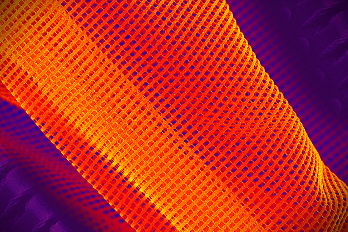
Metamaterials have unusual, useful, optical characteristics. Here we see a coloured electron-microscope image of a flexible mesh made of silver and magnesium fluoride. | Photo: John Rogers/University of Illinois/Science Photo Library
When a ray of light passes through a transparent material, its path is more complex than it seems. The wave pushes electrons back into the atoms of the material. The electric charge is momentarily disturbed and then returns to equilibrium, producing light that is indistinguishable from the original source. The phenomenon repeats itself from atom to atom through the material, until the wave escapes on the other side. What we perceive as a continuous flow is therefore more like a relay race. Moreover, at each stage, the angle of the light is slightly deviated: this is refraction, the same phenomenon that makes a rod half immersed in water appear broken.
Metamaterials work in a similar way. The difference is that they do not owe their properties to their atomic organisation, but to a completely artificial structure: layers of printed circuit boards on which patterns of copper, gold or silver are arranged at regular intervals, often referred to as ‘artificial atoms’.
By playing with the shape, size and arrangement of these patterns, scientists can selectively act on an electromagnetic wavelength – ultraviolet, visible light, infrared or microwave. They can also determine the amount of refraction produced. This will allow them to develop new imaging technologies and push back the physical resolution limits of conventional glass optics.
But miniaturisation remains a major obstacle: the printed patterns must be five to ten times smaller than the targeted wavelength. With a wavelength of around ten centimetres, microwaves do not pose any major problems. However, the most promising potential applications involve visible light with a wavelength of 390–780 nanometres. This requires the printing of patterns smaller than 100 nanometres – one thousandth the diameter of a human hair.
An alternative to hyperspectral cameras
“We don’t yet know how to make 3D nanostructures small and precise enough to interact effectively with visible light”, says Olivier Martin, the director of EPFL’s nanophotonics and metrology laboratory. This is why he works with two-dimensional surfaces, which are easier to produce. These metasurfaces are less efficient than a 3D material, but they still allow interesting manipulations of light.
One of these metamaterials is a glass substrate with a series of silver ‘u’-shaped patterns printed on it. The larger ones interact with red light and the smaller ones with blue light. By playing with the arrangement and shape of the patterns, a different refractive index can be induced for each colour. In other words, they can be focused at two very different points. “This separation effect is totally innovative, with no counterpart in conventional optics”, says Martin.
“This is certainly a significant advance in the field of metasurfaces”, says Juejun Hu, a materials scientist at the Massachusetts Institute of Technology (MIT), who was not involved in this project. “Unlike traditional optical devices and their broadband light deflection effect, this prototype can manipulate one colour, or a specific wavelength, without affecting the rest of the spectrum, which suggests many applications”.
Starting this autumn, Martin will team up with other EPFL scientists to explore potential applications for his metamaterials. For example, he imagines imaging devices for dermatology – to more easily identify certain ailments; for agriculture – to monitor crop growth and disease; and for hydrology. These are all processes that currently require specialised hyperspectral cameras.